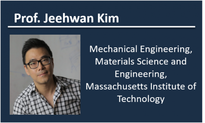

June 2025
3D heterogeneous integration, which involves vertically stacking wafers with embedded electronic devices, is emerging as the leading approach for augmenting the performance of electronics and optoelectronics. This method, however, demands complex procedures including creating through-silicon vias (TSVs), filling these vias with copper, and bonding the wafers via micro-bumps or Cu hybrid bonding. Eliminating the use of wafers in this complex 3D assembly, a.k.a. monolithic 3D (M3D), could streamline the process and reduce the length of data paths. Yet, current technologies scarcely allow for the removal and reassembly of active single-crystalline devices from wafers. Moreover, directly epitaxial growths onto existing circuits present additional hurdles. Over the last decade, my group at MIT has pioneered epitaxy techniques for advancing wafer-free M3D integration of single-crystalline semiconductor devices. Firstly, I will introduce our innovation in transfer-based M3D integration of single-crystalline devices based on remote epitaxy [1-7]. Secondly, I will introduce our recent development of growth-based M3D integration by successfully implementing single-crystalline channel material growths directly on integrated circuits at a BEOL compatible temperature [8-9]. This really unlocks the way to seamless monolithic integration for advanced 3D logic/memory and AI systems.
References: [1] Nature 544, 340 (2017), [2] Nature Materials 17, 999 (2018), [3] Nature Materials 18, 550 (2019), [4] Nature Nanotechnology 15, 272-276 (2020), [5] Nature, 578, 75 (2020), [6] Nature, 614, 81 (2023), [7] Nature Electronics, 5, 386 (2022), [8] Nature, 614, 88 (2023), [9] Nature (2024)
